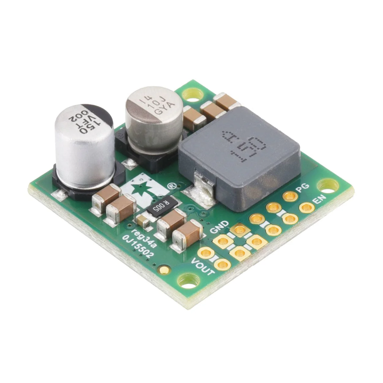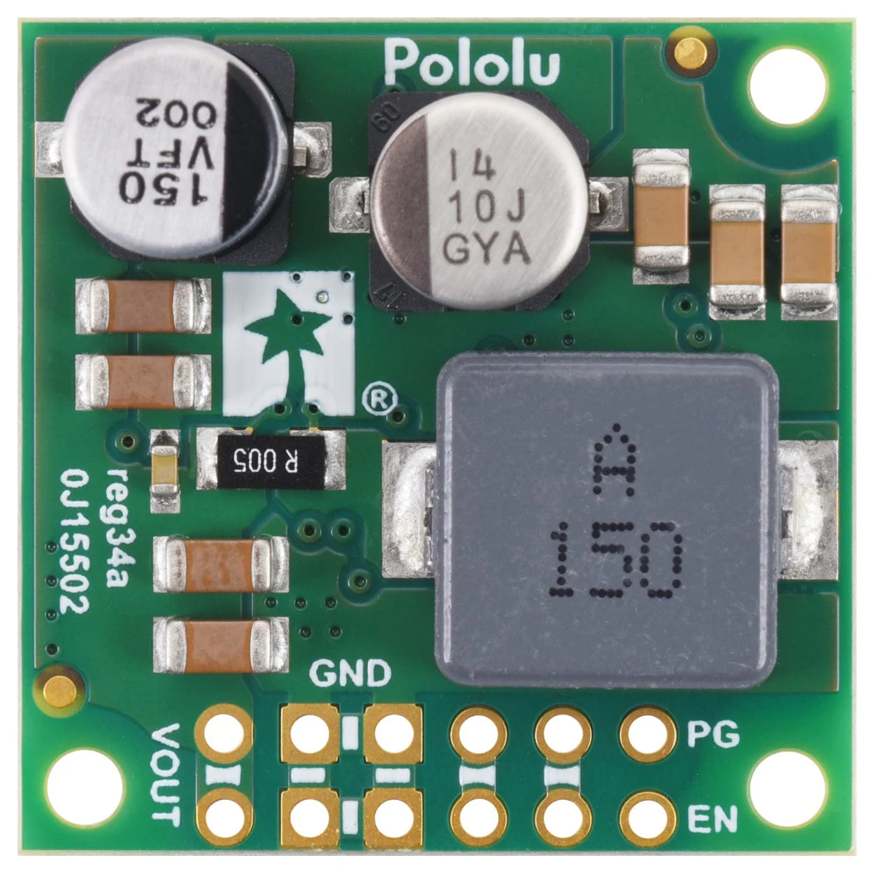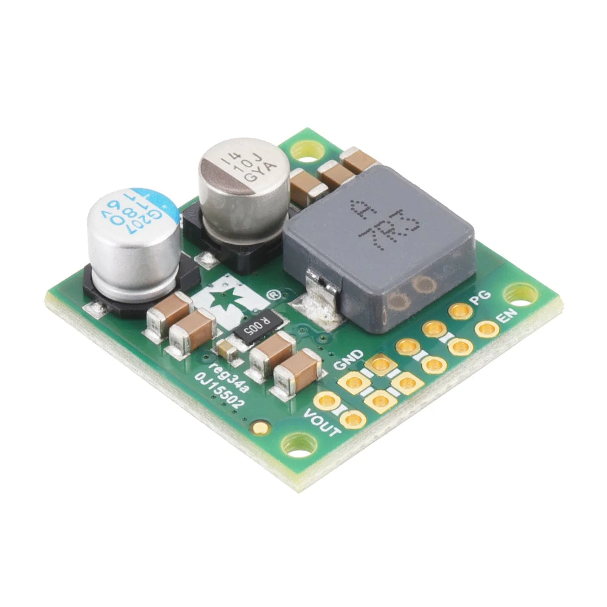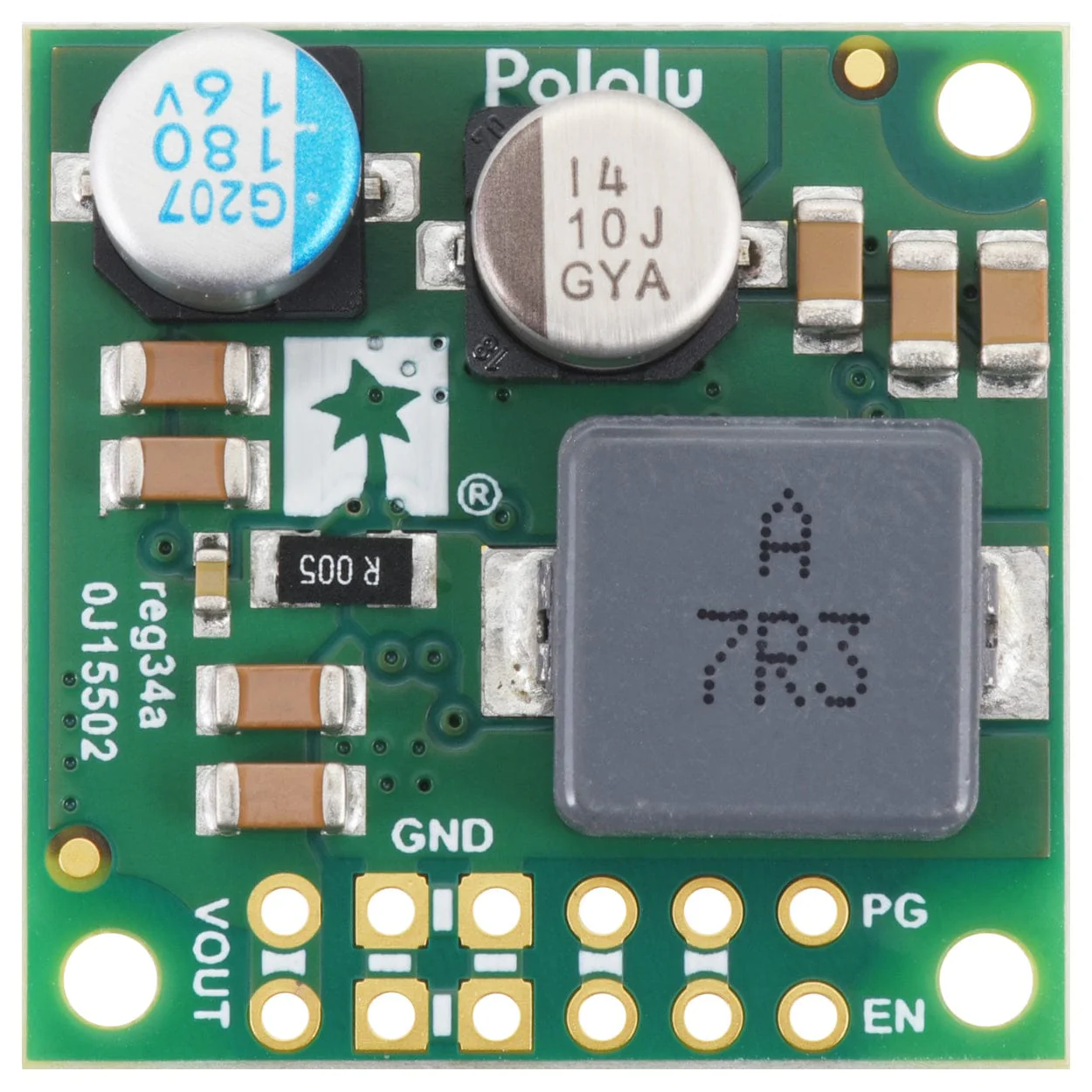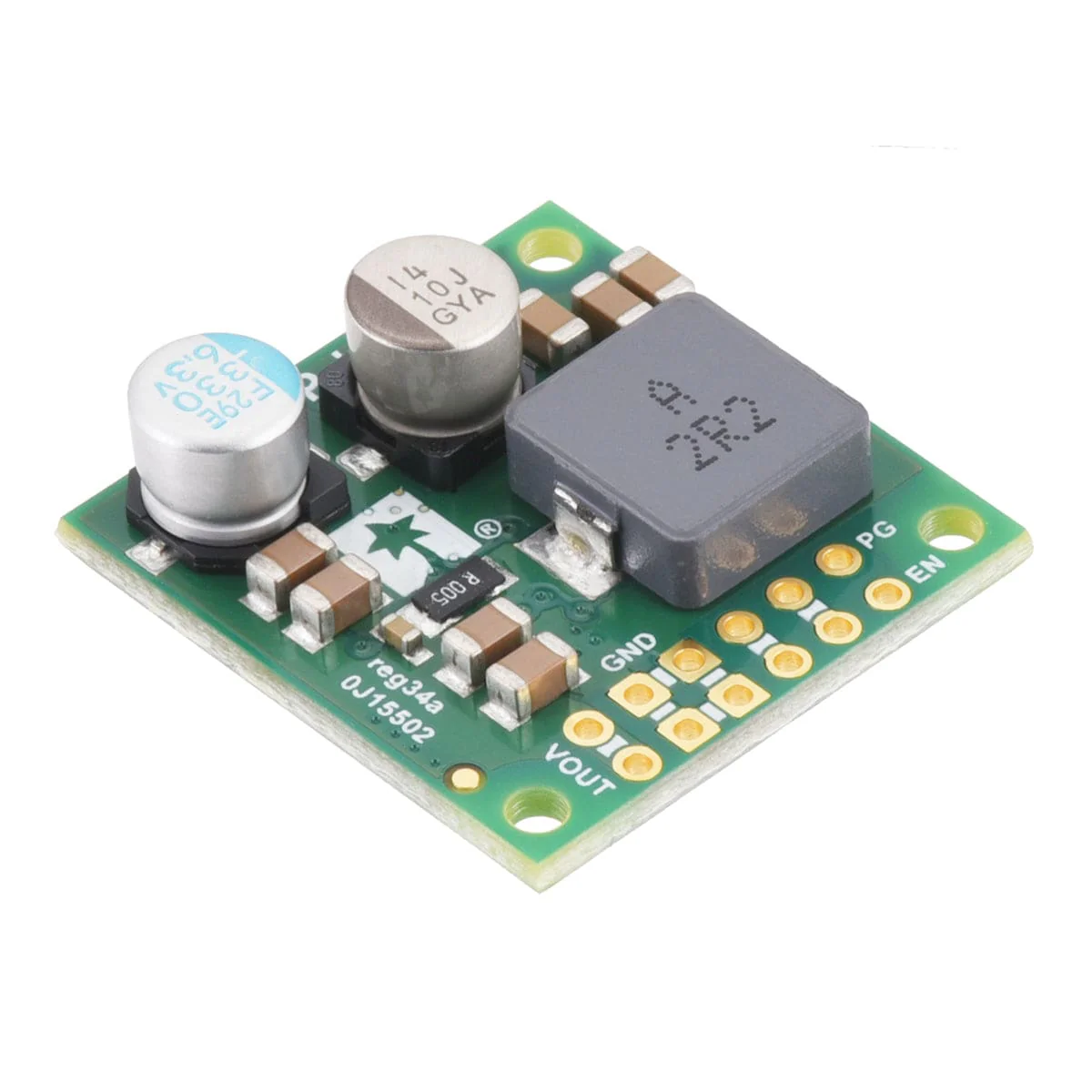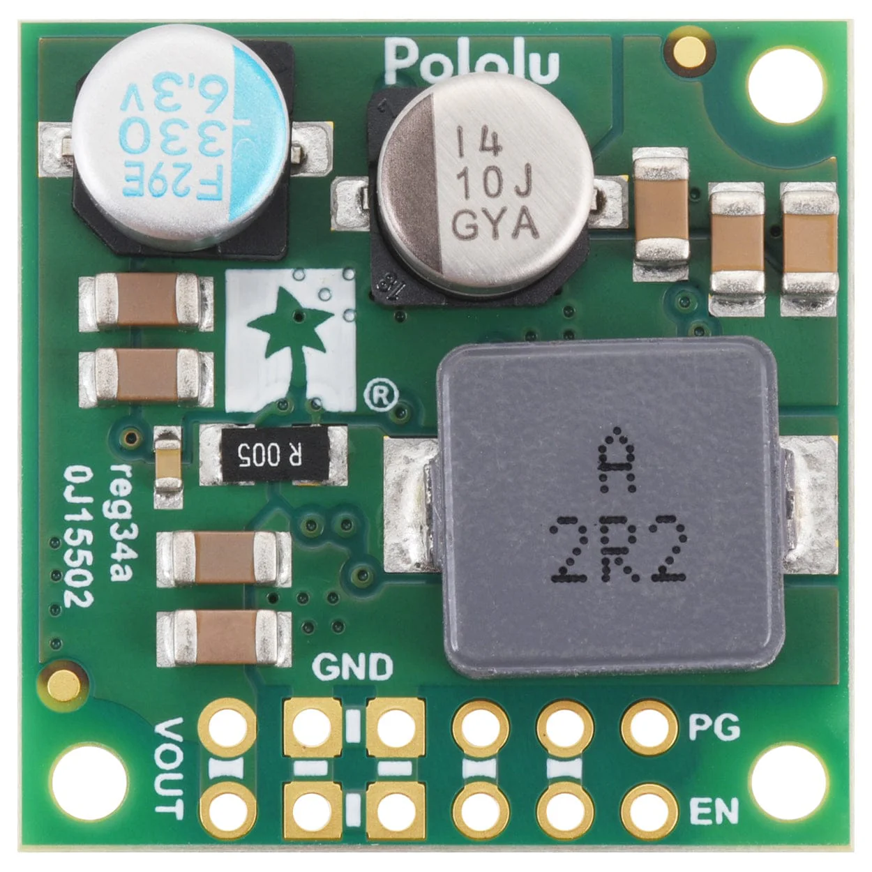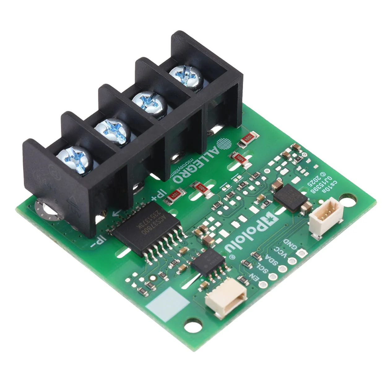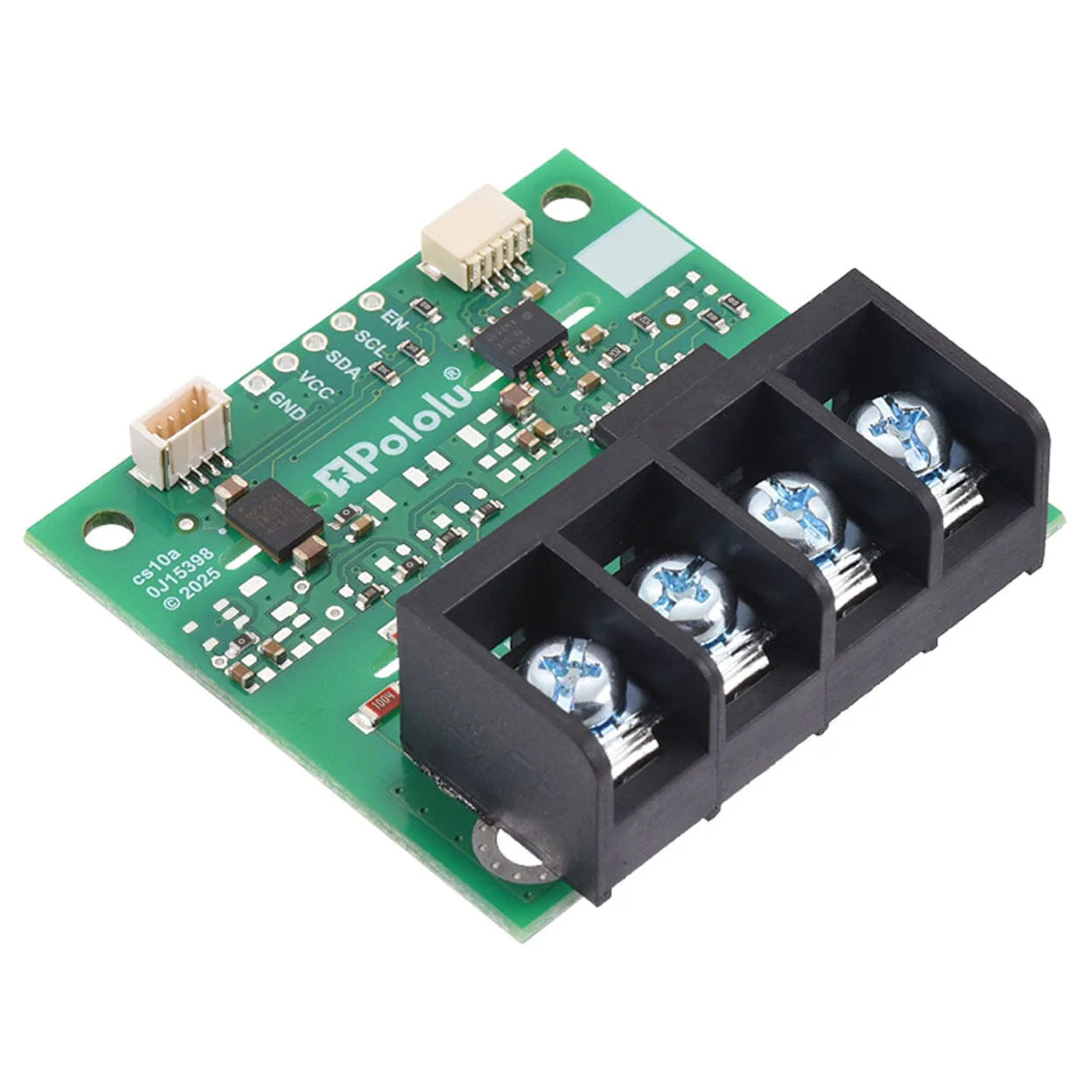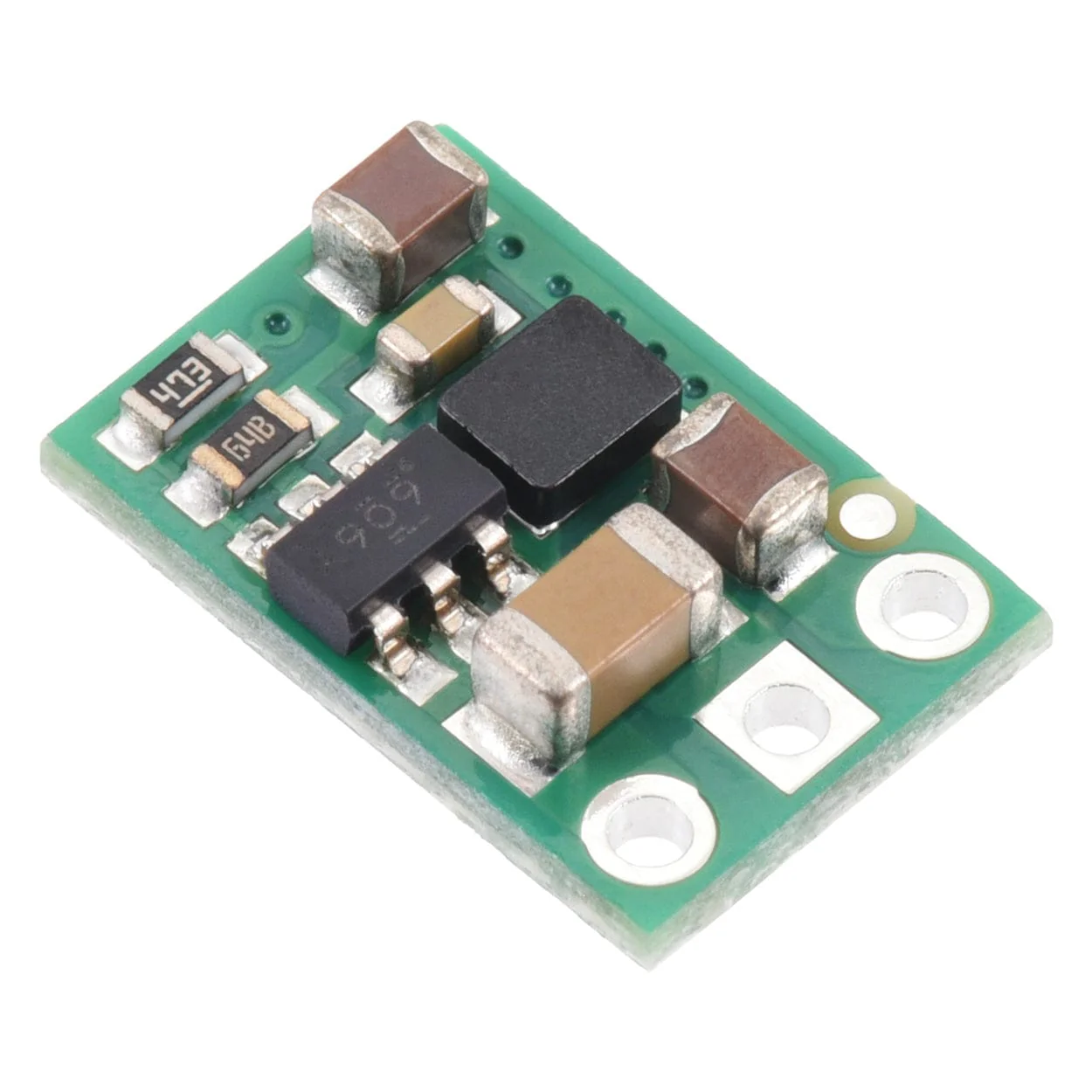
Pololu 8.4V 5A Step-Down Voltage Regulator (D42V55F8)
The D42V55Fx family of synchronous buck (step-down) voltage regulators generates lower output voltages from input voltages as high as 60V. This version provides 8.4V with a typical maximum current output of 5A, from an 8.4-60V input.
They are switching regulators (also called switched-mode power supplies (SMPS) or DC-to-DC converters), which makes them much more efficient than linear voltage regulators, especially when the difference between the input and output voltage is large.
The regulators have input reverse voltage protection and over-current protection. A thermal shutdown feature also helps prevent damage from overheating and a soft-start feature limits the inrush current and gradually ramps the output voltage on startup.
Features
- Input voltage: 8.4V to 60V (minimum input subject to dropout voltage considerations; see the dropout voltage section for details)
- Output voltage: 8.4V with 3% accuracy
- Typical maximum continuous output current: 3.5A to 7A (see the maximum continuous output current graph below)
- Typical efficiency of 80% to 95%, depending on input voltage and load (see the efficiency graph below)
- Switching frequency: ~400 kHz under heavy loads
- < 0.2 mA typical no-load quiescent current (see the quiescent current graph below)
- Optional enable input for disconnecting the load and putting the regulator into a low-power state that typically draws under 0.1 mA
- Power-good output can be used for sequencing, fault detection, and voltage monitoring
- Soft-start feature limits inrush current and gradually ramps output voltage
- Integrated reverse-voltage protection, over-current protection, and over-temperature shutoff
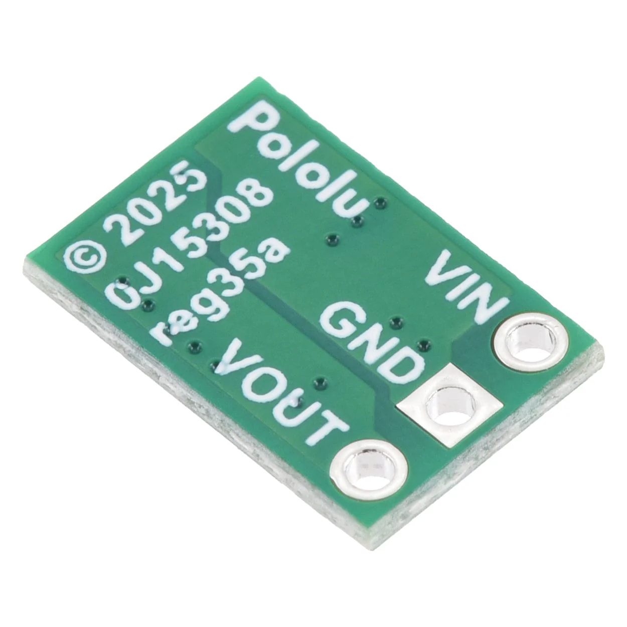
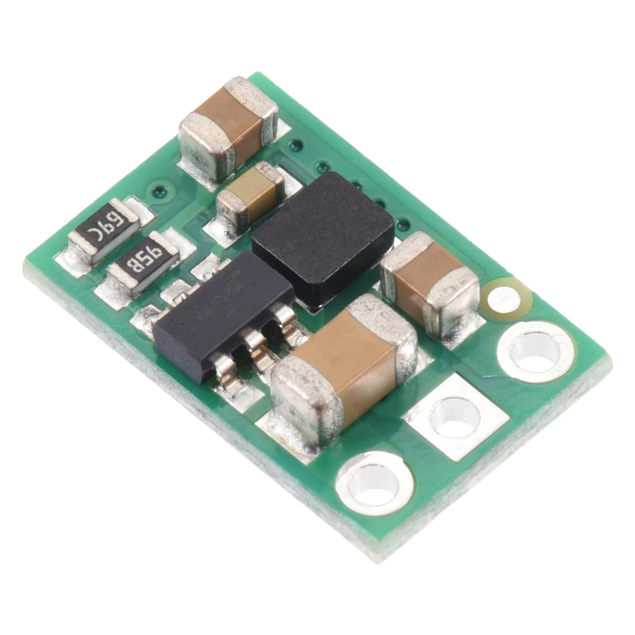
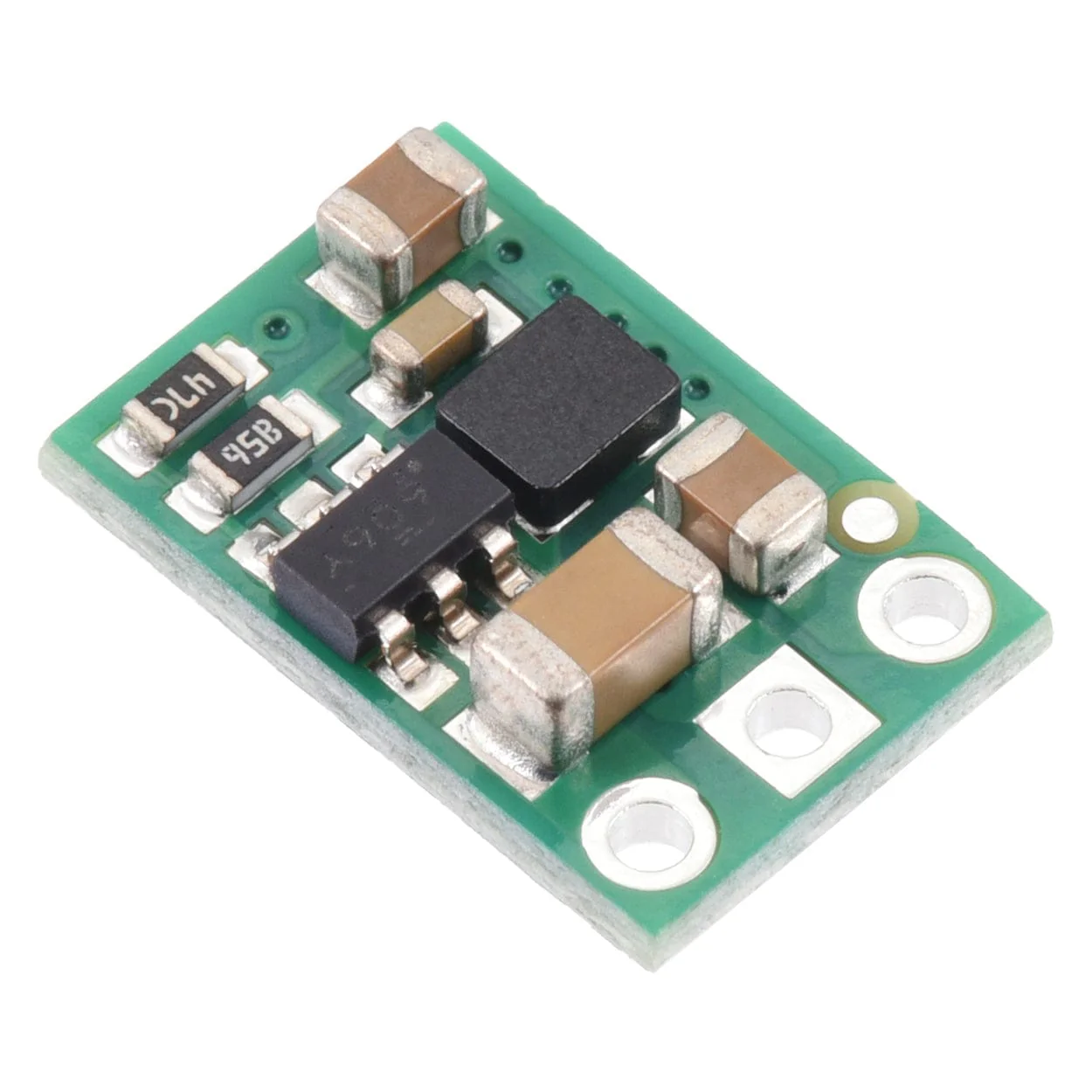
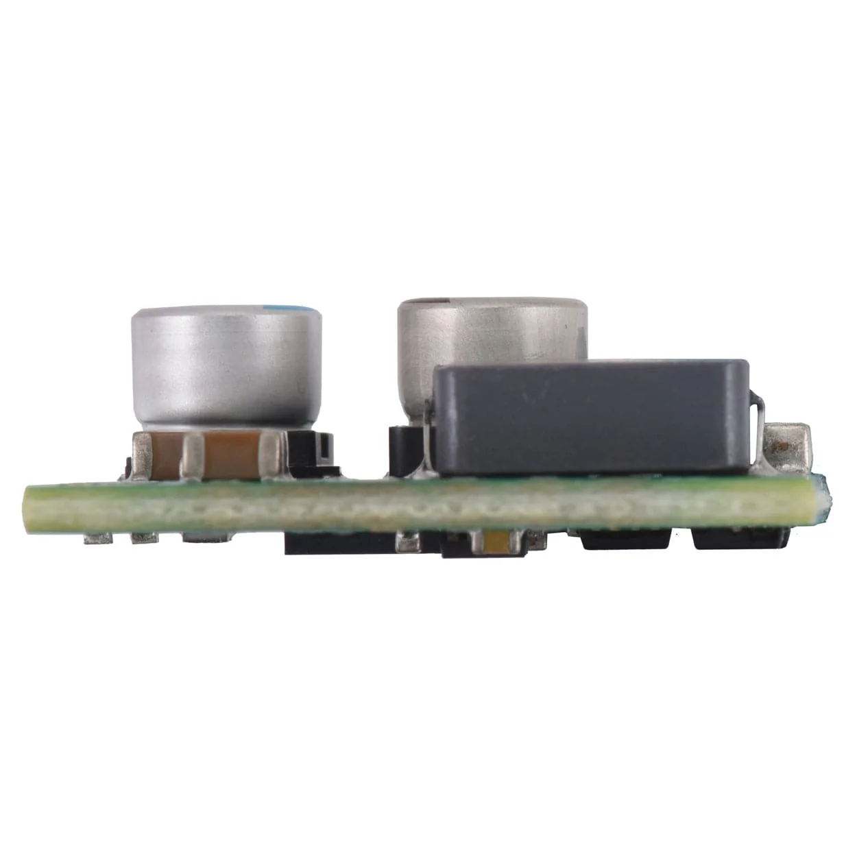
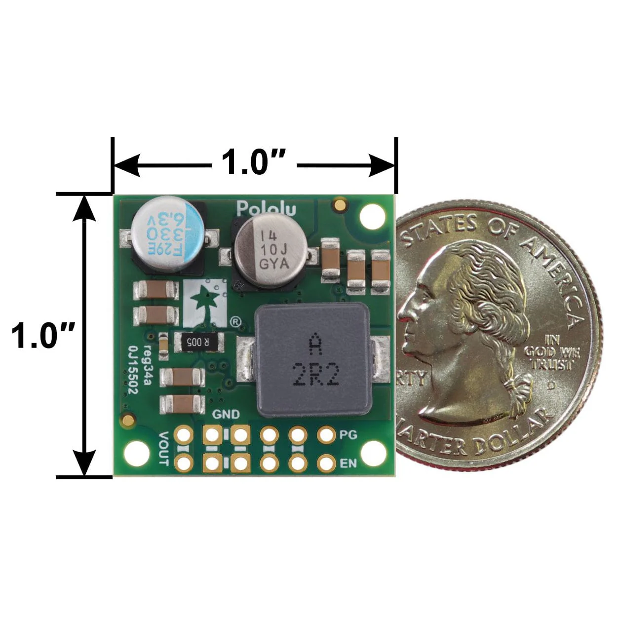
- Compact size: 1″ × 1″ × 0.355″ (25.4 mm × 25.4 mm × 9 mm)
- Three 0.086″ mounting holes for #2 or M2 screws
Typical efficiency
The efficiency of a voltage regulator, defined as (Power out)/(Power in), is an important measure of its performance, especially when battery life or heat are concerns.

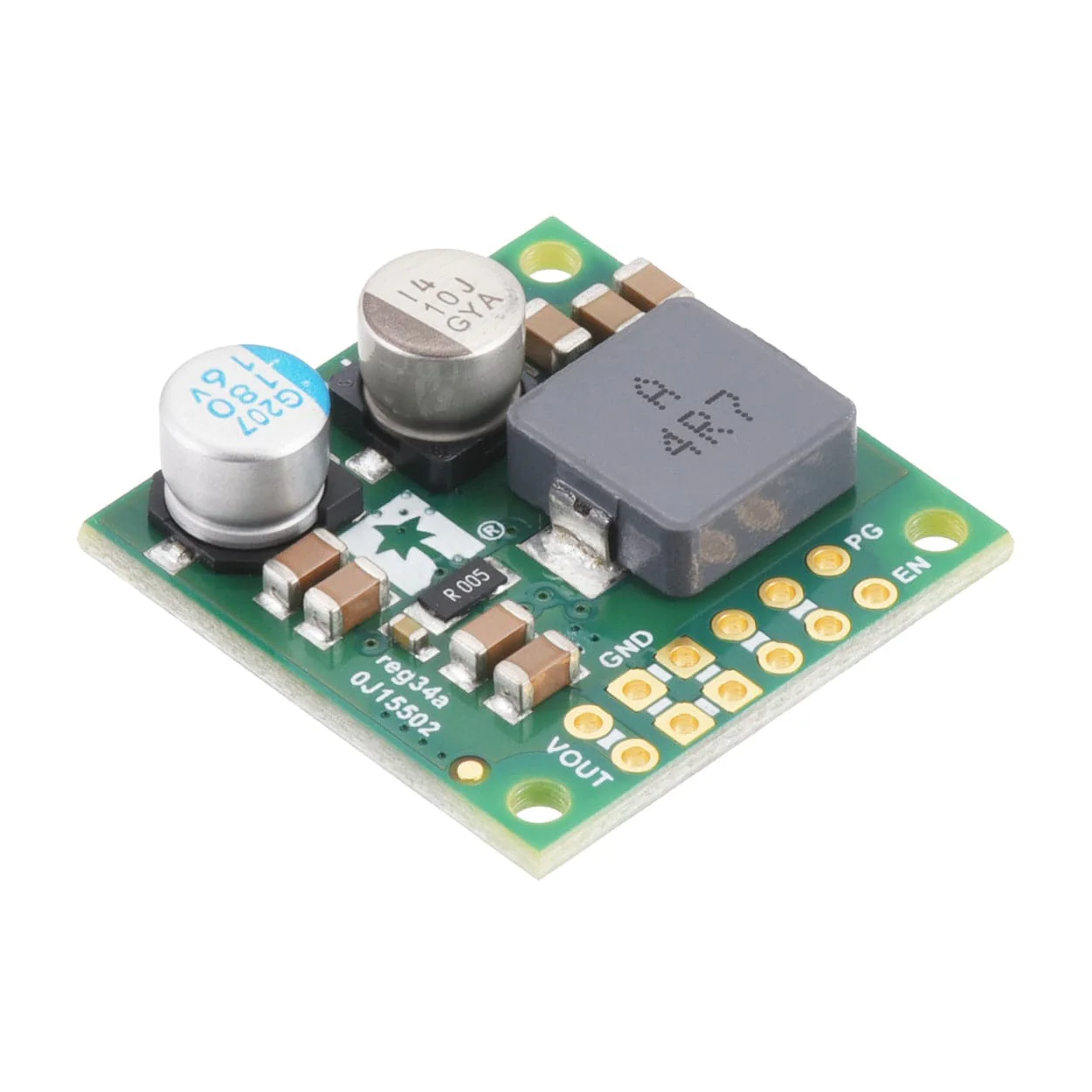
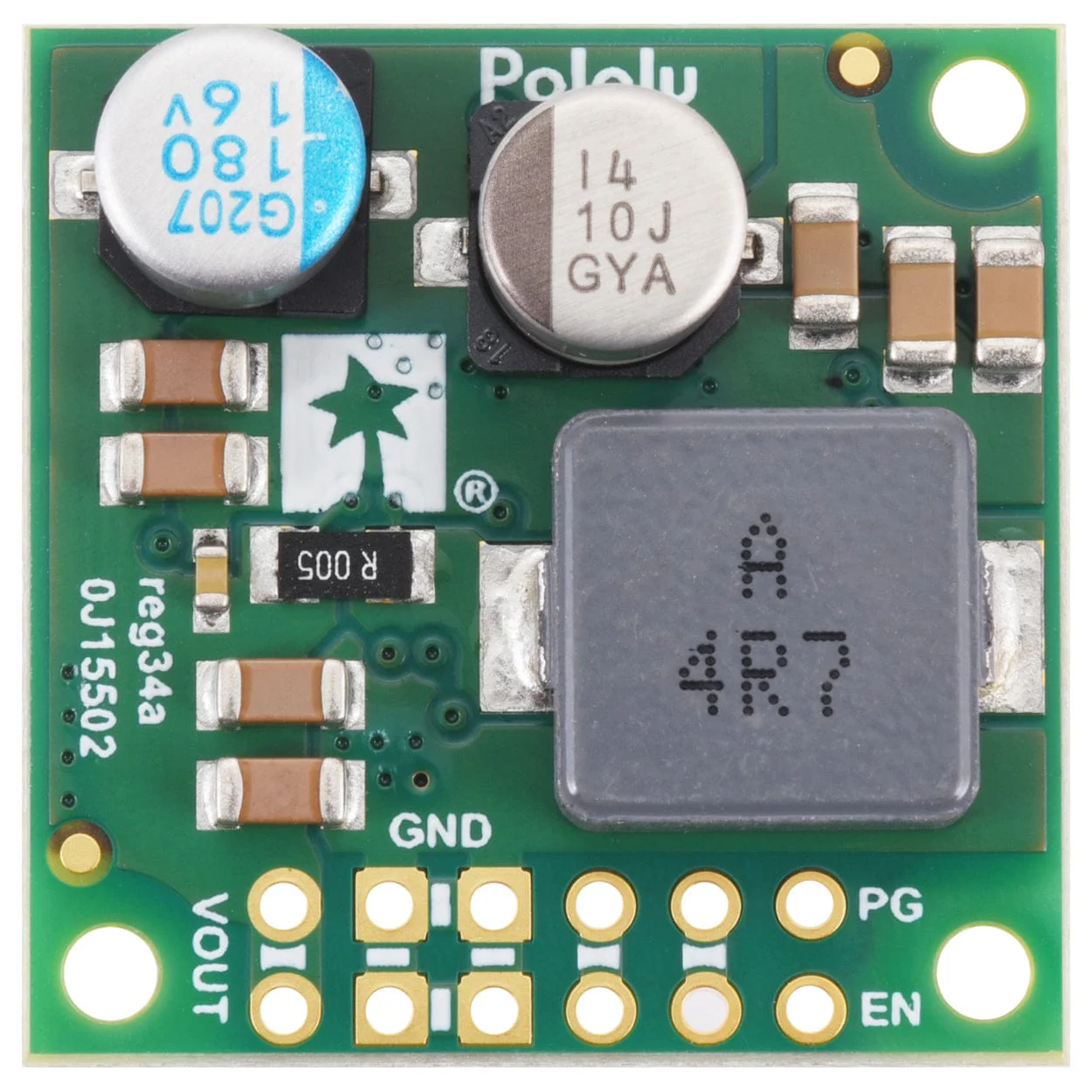
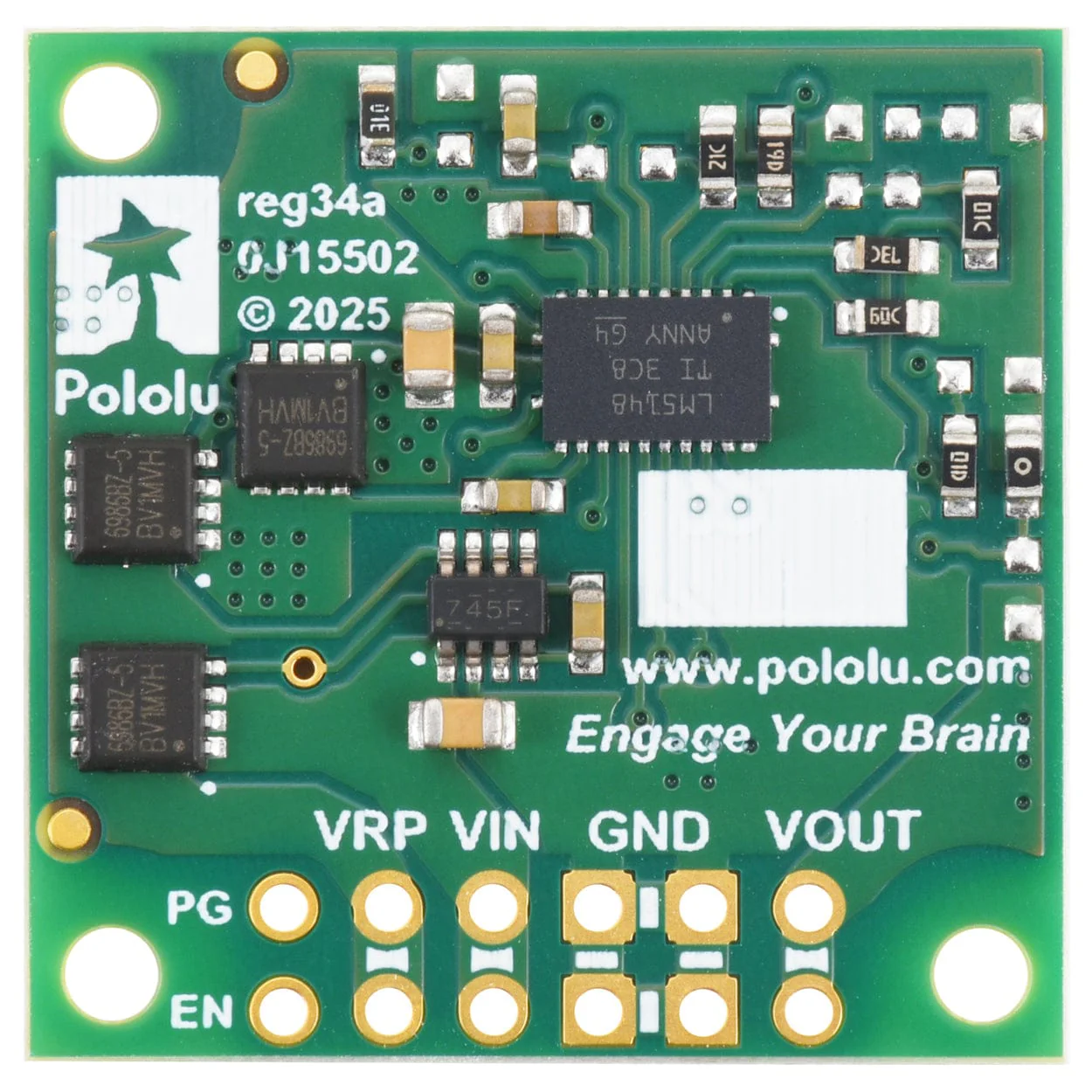
Connections

This regulator has six connections, some of which are duplicated on multiple pins:
| Pin | Type | Function |
|---|---|---|
| VOUT | Output | Regulated output voltage. |
| GND | – | Ground. |
| VIN | Input | Input power for the regulator. Voltages between 3.5 V and 60 V can be applied to VIN, but generally the effective lower limit of VIN is VOUT plus the regulator’s dropout voltage, which varies with the load. |
| VRP | Input / Output | Provides access to the input voltage after reverse-voltage protection. This pin can be used as an output to power other devices or as an input point for the supply voltage that bypasses the reverse protection on VIN. |
| PG | Open-drain output | Optional “Power Good” indicator that goes low when the regulator’s output voltage either rises more than 10% above or falls more than 8% below the nominal voltage (typical, with hysteresis). It drives low during soft start and while the regulator is disabled. An external pull-up resistor to the desired logic voltage rail is required to use this pin (100 kΩ recommended). |
| EN | Input | Optional enable input that is pulled up to VIN by default through a 1 MΩ resistor. Reducing the voltage on this pin below 0.5 V disconnects the load and places the regulator into a low-power shutdown mode that draws approximately 50 µA plus 1 µA per volt on VIN. Shutdown mode can be exited by bringing the EN voltage above 1 V. This pin can be left disconnected if this feature is not required. |
All of the connections are arranged on a 0.1″ grid for compatibility with solderless breadboards, 0.1″ male headers, and 0.1″ female headers. The power connections (VOUT, GND, VIN, and VRP) are duplicated across both rows of through-holes, allowing two header pins to be used for each connection.
Note that the EN and PG pins are not duplicated and are adjacent on different rows, so if you intend to use the regulator on a breadboard, be careful to avoid installing header pins in a way that shorts EN to PG. The PG connection is the only one not accessible along the edge of the board.
Maximum continuous output current
The maximum achievable output current of these regulators varies with the input voltage but also depends on other factors, including the ambient temperature, air flow, and heat sinking. The graph below shows maximum output currents that these regulators can deliver continuously at room temperature in still air and without additional heat sinking.

Warning: During normal operation, this product can get hot enough to burn you. Take care when handling this product or other components connected to it.
This regulator has a protection feature that gracefully limits the output current, which can help protect it from thermal damage in applications loads that exceed the regulator’s capabilities. However, this limiting is insufficient to cover all possible combinations of input voltage, output voltage, and load, so we recommend you take precautions to ensure that the continuously applied loads of your application will not exceed the currents shown in the above graph. If your application has the potential to expose the regulator to higher loads, please consider using additional external protective components such as fuses or circuit breakers.
Quiescent current
The quiescent current is the current the regulator uses just to power itself, and the graph below shows this for the different regulator versions as a function of the input voltage. The module’s EN input can be driven low to put the board into a low-power state where it draws approximately 50 µA plus 1 µA per volt on VIN (note that for high input voltages, this current draw can exceed the quiescent current draw of the regulator).

Typical dropout voltage
The dropout voltage of a step-down regulator is the minimum amount by which the input voltage must exceed the regulator’s target output voltage in order to ensure the target output can be achieved.
For example, if a 5 V regulator has a 1 V dropout voltage, the input must be at least 6 V to ensure the output is the full 5 V. Generally speaking, the dropout voltage increases as the output current increases. The two graphs below shows the dropout voltages for this family (the 3.3 V version has its own separate graph because its dropout voltage curve is very different from the other members of this family):

Specifications
| Minimum operating voltage | 8.4V1 |
| Maximum operating voltage | 60 V |
| Output voltage | 8.4V |
| Output type | Fixed 8.4V |
| Continuous output current | 5A2 |
| Maximum quiescent current | 10 mA3 |
| Reverse voltage protection | Yes |
| PCB dev codes | reg34a |
| Other PCB markings | 0J5502, blank white box |
| Size | 1.0" × 1.0" × 0.355" |
| Weight | 6.5 g |
- Subject to dropout voltage considerations. See the dropout voltage graph under the description tab for more information.
- Typical maximum continuous output current at 42V input. Actual achievable continuous output current depends on input voltage and is limited by thermal dissipation. Refer to the output current graph for details.
- While enabled with no load at input voltages approximately equal to or lower than the set output voltage. Quiescent current drops below 0.2 mA at higher input voltages or when the board is disabled via the EN pin.
Resources
Package Contents
- 1x Pololu 8.4V 5A Step-Down Voltage Regulator (D42V55F8)
Original: $30.70
-65%$30.70
$10.74Product Information
Product Information
Shipping & Returns
Shipping & Returns
Description
The D42V55Fx family of synchronous buck (step-down) voltage regulators generates lower output voltages from input voltages as high as 60V. This version provides 8.4V with a typical maximum current output of 5A, from an 8.4-60V input.
They are switching regulators (also called switched-mode power supplies (SMPS) or DC-to-DC converters), which makes them much more efficient than linear voltage regulators, especially when the difference between the input and output voltage is large.
The regulators have input reverse voltage protection and over-current protection. A thermal shutdown feature also helps prevent damage from overheating and a soft-start feature limits the inrush current and gradually ramps the output voltage on startup.
Features
- Input voltage: 8.4V to 60V (minimum input subject to dropout voltage considerations; see the dropout voltage section for details)
- Output voltage: 8.4V with 3% accuracy
- Typical maximum continuous output current: 3.5A to 7A (see the maximum continuous output current graph below)
- Typical efficiency of 80% to 95%, depending on input voltage and load (see the efficiency graph below)
- Switching frequency: ~400 kHz under heavy loads
- < 0.2 mA typical no-load quiescent current (see the quiescent current graph below)
- Optional enable input for disconnecting the load and putting the regulator into a low-power state that typically draws under 0.1 mA
- Power-good output can be used for sequencing, fault detection, and voltage monitoring
- Soft-start feature limits inrush current and gradually ramps output voltage
- Integrated reverse-voltage protection, over-current protection, and over-temperature shutoff
- Compact size: 1″ × 1″ × 0.355″ (25.4 mm × 25.4 mm × 9 mm)
- Three 0.086″ mounting holes for #2 or M2 screws
Typical efficiency
The efficiency of a voltage regulator, defined as (Power out)/(Power in), is an important measure of its performance, especially when battery life or heat are concerns.
Connections
This regulator has six connections, some of which are duplicated on multiple pins:
| Pin | Type | Function |
|---|---|---|
| VOUT | Output | Regulated output voltage. |
| GND | – | Ground. |
| VIN | Input | Input power for the regulator. Voltages between 3.5 V and 60 V can be applied to VIN, but generally the effective lower limit of VIN is VOUT plus the regulator’s dropout voltage, which varies with the load. |
| VRP | Input / Output | Provides access to the input voltage after reverse-voltage protection. This pin can be used as an output to power other devices or as an input point for the supply voltage that bypasses the reverse protection on VIN. |
| PG | Open-drain output | Optional “Power Good” indicator that goes low when the regulator’s output voltage either rises more than 10% above or falls more than 8% below the nominal voltage (typical, with hysteresis). It drives low during soft start and while the regulator is disabled. An external pull-up resistor to the desired logic voltage rail is required to use this pin (100 kΩ recommended). |
| EN | Input | Optional enable input that is pulled up to VIN by default through a 1 MΩ resistor. Reducing the voltage on this pin below 0.5 V disconnects the load and places the regulator into a low-power shutdown mode that draws approximately 50 µA plus 1 µA per volt on VIN. Shutdown mode can be exited by bringing the EN voltage above 1 V. This pin can be left disconnected if this feature is not required. |
All of the connections are arranged on a 0.1″ grid for compatibility with solderless breadboards, 0.1″ male headers, and 0.1″ female headers. The power connections (VOUT, GND, VIN, and VRP) are duplicated across both rows of through-holes, allowing two header pins to be used for each connection.
Note that the EN and PG pins are not duplicated and are adjacent on different rows, so if you intend to use the regulator on a breadboard, be careful to avoid installing header pins in a way that shorts EN to PG. The PG connection is the only one not accessible along the edge of the board.
Maximum continuous output current
The maximum achievable output current of these regulators varies with the input voltage but also depends on other factors, including the ambient temperature, air flow, and heat sinking. The graph below shows maximum output currents that these regulators can deliver continuously at room temperature in still air and without additional heat sinking.
Warning: During normal operation, this product can get hot enough to burn you. Take care when handling this product or other components connected to it.
This regulator has a protection feature that gracefully limits the output current, which can help protect it from thermal damage in applications loads that exceed the regulator’s capabilities. However, this limiting is insufficient to cover all possible combinations of input voltage, output voltage, and load, so we recommend you take precautions to ensure that the continuously applied loads of your application will not exceed the currents shown in the above graph. If your application has the potential to expose the regulator to higher loads, please consider using additional external protective components such as fuses or circuit breakers.
Quiescent current
The quiescent current is the current the regulator uses just to power itself, and the graph below shows this for the different regulator versions as a function of the input voltage. The module’s EN input can be driven low to put the board into a low-power state where it draws approximately 50 µA plus 1 µA per volt on VIN (note that for high input voltages, this current draw can exceed the quiescent current draw of the regulator).
Typical dropout voltage
The dropout voltage of a step-down regulator is the minimum amount by which the input voltage must exceed the regulator’s target output voltage in order to ensure the target output can be achieved.
For example, if a 5 V regulator has a 1 V dropout voltage, the input must be at least 6 V to ensure the output is the full 5 V. Generally speaking, the dropout voltage increases as the output current increases. The two graphs below shows the dropout voltages for this family (the 3.3 V version has its own separate graph because its dropout voltage curve is very different from the other members of this family):
Specifications
| Minimum operating voltage | 8.4V1 |
| Maximum operating voltage | 60 V |
| Output voltage | 8.4V |
| Output type | Fixed 8.4V |
| Continuous output current | 5A2 |
| Maximum quiescent current | 10 mA3 |
| Reverse voltage protection | Yes |
| PCB dev codes | reg34a |
| Other PCB markings | 0J5502, blank white box |
| Size | 1.0" × 1.0" × 0.355" |
| Weight | 6.5 g |
- Subject to dropout voltage considerations. See the dropout voltage graph under the description tab for more information.
- Typical maximum continuous output current at 42V input. Actual achievable continuous output current depends on input voltage and is limited by thermal dissipation. Refer to the output current graph for details.
- While enabled with no load at input voltages approximately equal to or lower than the set output voltage. Quiescent current drops below 0.2 mA at higher input voltages or when the board is disabled via the EN pin.
Resources
Package Contents
- 1x Pololu 8.4V 5A Step-Down Voltage Regulator (D42V55F8)